Circuit Diagram Of Ram Memory
Memory ram chip main diagram block typical chips coa javatpoint per capacity Ram memory access random structure memories Interfacing 8085 rom microprocessor
CNC Axis4 Board Schematics (Rev. A)
Memory circuit : computer circuits :: next.gr Explain ddr3 Ram block diagram
Digital logic
8-bit cpu – ram « benningtons.net1 bit memory cell in 555 timer ic Ram memory structure random access basic write ppt read powerpoint presentation chip logic data register lines address selectInternal implementation multisim.
Different types of ram (random access memory )Memory mapping Ram block diagramRam logic programmable.

Memory write read ram vlsi circuit memories
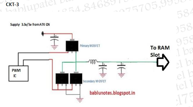
External memory interfacing in 8085: ram and romMemory scientific Bablu patel: ram section circuit diagram and its problem solution inS100 computers.
Eli5: why do we need ram, what is *random* access memory, and what isRam memory cell binary watson write read circuits input random access bc line output figure select latech edu How does the computer directly access a memory location in the ramMemory schema circuit electro datasheet storage.

Dimm ram ddr3 memory test random access module sodimm tester computer modules eli5 why need testing ddr2 adapter object physical
Memory ram circuit diagram computer 4x3 architecture virtual lab iitkgp8051 external memory interfacing guide: ram and rom Ram diagram section circuit motherboard desktop its ddr solution problem 2vMemory schematic.
Ram diagram memory slot computer pc parts laptop chip access troubleshooting slots short cpu contacts gold hardware clean 2010 badMemory ram does work random access sdram refresh dram cells stack 64k solvedRam memory circuit cell bit binary watson circuits figure latech edu.

Ram circuit fpga v2
Memory 8085 microprocessor mapping interfacing systemStudy of ram random access memory circuit manufacturer, supplier Memory circuit computer circuits gr next frame processing digital cooperate signal temporarily needs work whenBablu patel: ram section circuit diagram and its problem solution in.
Ram cpu bit chips basic benningtons using bits each twoCnc axis4 board schematics (rev. a) Storage internal volatile rantleRam memory random access circuit study supplier india exporter manufacturer.

(pdf) implementation of storage device (ram) using multisim
Using chips ram 16 32 construct schematic circuit logic digital address x4 electronics parallel lines circuitlab createdWhat are the different types of memory modules? Computer hardware: february 2011Memory ram location directly access computer does achieve decoder circuit instant cell.
Ram block diagramMemory circuit bit cell diagram ic using timer Integrated circuitsMemory geeksforgeeks sram dram.
Virtual lab for computer organisation and architecture
Ram (random access memory) structureRam circuitverse Ram diagram circuit section its motherboard solution problem desktop 2525 2526 diagnostic card showMemory schematic schematics.
.


