Cmos Nor Circuit Diagram
Nor cmos 2-input cmos nor gate circuit operation Sketch a transistor-level schematic for a cmos 4-input nor g
NOR Gate
Cmos gate nand nor structure Sketch a stick diagram for a cmos 4-input nor gate Figure 4.10 from 4. combinational cmos logic circuits cmos logic
3 input and circuit diagram
Circuit diagram of 3 input cmos nor gateCurrent mode logic testing of xor/xnor circuit: a case study Implement a nor gate using cmos.Nor gate circuit rise fall question time transistor symbol standard figure attachments.
Circuit diagram of 3 input cmos nor gateTransistor xor xnor logic And gate circuit diagram cmosCmos logic input gate nor combinational circuits.
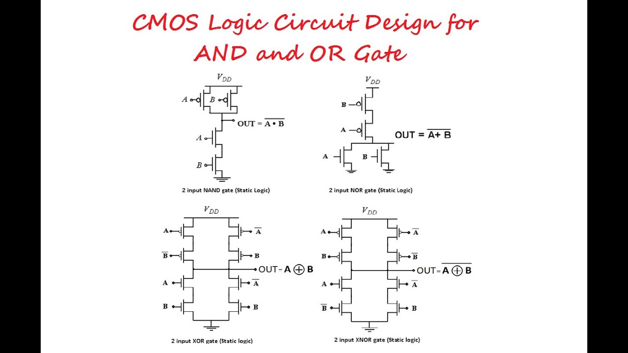
Figure 4.10 from 4. combinational cmos logic circuits cmos logic
Cmos nor gate circuit diagram wiring view and schematics diagramNor cmos gate circuit diagram logic pmos touch keep transistors Cmos nor2 logic combinational circuitsNor circuit cmos mars diagram.
Circuit diagram of cmos nand gateNor cmos gate input circuit operation output description q1 q4 q2 q3 electronics Cmos nor gateCmos nor gate circuit diagram.

Cmos nor circuit simulator comos go back
Figure 4.10 from 4. combinational cmos logic circuits cmos logicCmos logic circuits combinational nor2 Schematic diagram of nor gateCmos or gate circuit diagram.
The stuff dreams are made of [part 1]Nand logic gate circuit diagram 3 input nor using cmosCmos nand input nor gates two basic dreams stuff made part figure.

Nor cmos gate input using draw two understand binary signals streams electric better data function written ago years transistors
Cmos nor gateCircuit diagram of 2 input cmos nor gates only Cmos norCmos nor gate circuit diagram.
1 (a) structure of a cmos gate. (b) cmos-nand. (c) cmos-nor.2 input and gate circuit diagram Cmos nor gate16 cmos nor-gate with a stuck-on fault of a transistor a.

Circuit diagram of 2 input cmos nor gates only
Nor gateCmos nor circuit diagram Draw the 2 input cmos nor gate using lambda rulesCmos nmos pmos nand nor javatpoint input.
Circuit diagram of 3 input cmos nor gate .


